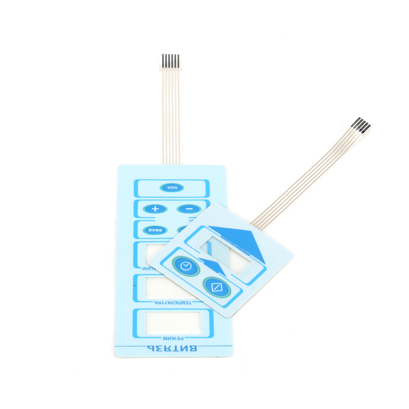
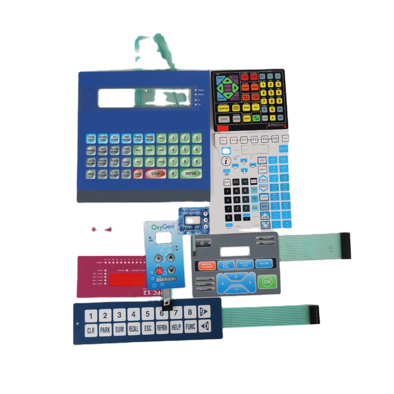
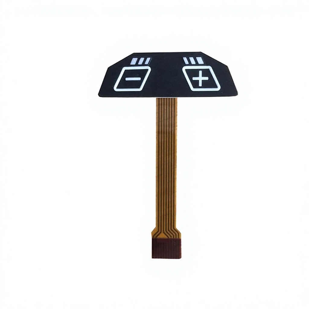
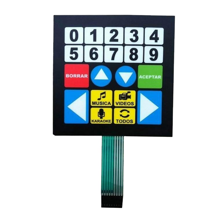
Featured Printed Membrane Switches & Circuits
Explore our top-tier tactile interfaces, custom-tailored for medical instruments, industrial automation consoles, and mission-critical electronics.
29+
Years Engineering Expertise
5,000m²
Modern Cleanroom Facility
100%
Electrical & Optical Testing
50%+
Export Ratio (EU, US, APAC)

Intertek Onsite Verified Manufacturer & Assessed Supplier
Full compliance validation for ISO9001 quality management, cleanroom manufacturing, RoHS and REACH environmental directives.
Why Global Tier-1 OEMs Partner with Us
Zhejiang ZIRA Membrane Switch Co., Ltd. brings decades of advanced precision printing, mechanical engineering, and microelectronics bonding into every production batch.
Vertical In-House Integration
From screen plate production, polymeric conductive silver paste formulation, precision flatbed printing, and micro-embossing to Class 10,000 cleanroom lamination, we eliminate outsourcing dependencies to deliver competitive cost structures.
Rigorous 100% Quality Assurance
Zero micro-opens, zero latent resistance spikes. Every single membrane trace undergoes computerized automated test scanning for loop resistance, contact bounce, breakdown voltage, insulation barrier (>100MΩ at 100V DC), and snap ratio feel.
Rapid DFM & Agile Prototyping
Accelerate your NPI (New Product Introduction) cycles. Our engineering team conducts comprehensive Design for Manufacturability (DFM) analyses within 24 hours, shipping production-grade validation prototypes in 3 to 7 working days.
Proven Enterprise Provenance
Trusted over decades by global leaders in industrial automation and power grid distribution including ABB and Emerson. We maintain long-term international trade contracts and complete supply traceability.
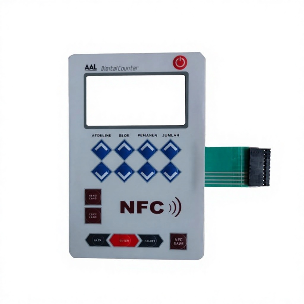
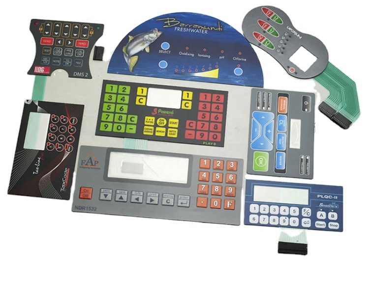
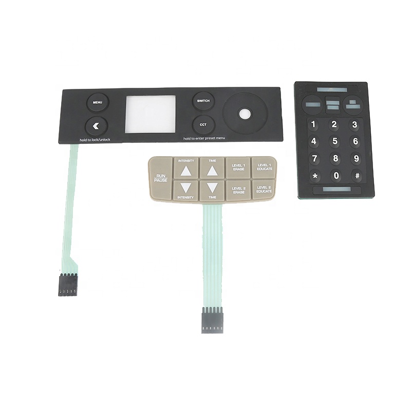
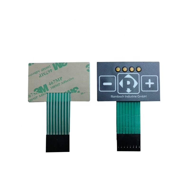
Technical Architecture: High-Reliability Printed Membrane Circuits
Modern printed membrane circuits are no longer simple electrical momentary closures; they are mission-critical interconnect platforms serving as the sensory boundary between operators and complex electronic systems. In harsh operating scenarios—such as high electromagnetic noise floors, continuous chemical sanitation in operating rooms, or wide-spectrum ambient temperature cycling—the engineering configuration of the multilayer stack-up determines system survivability.
At ZIRA, our conductive silver trace deposition utilizes proprietary fine-line screen printing technology achieving line widths and spacings down to 0.25mm (10 mil) with exceptional edge definition. To prevent electromigration—a catastrophic failure mode where silver ions migrate across insulating spaces under humid DC bias—our circuits integrate a printed pinhole-free carbon overcoat or UV dielectric mask that encapsulates the conductor traces completely.
| Layer Architecture | Typical Materials | Functional Performance Criteria |
|---|---|---|
| 1. Graphic Overlay | Autotype XE/Fine Polyester (PET) or Polycarbonate (PC) (0.125mm - 0.25mm) | Sub-surface back-printing; chemical resistance to isopropyl alcohol, bleach, and petrochemical solvents; UV stability rating up to 5+ years. |
| 2. Overlay Adhesive | 3M 467MP, 3M 468MP, or 3M 300LSE low-surface-energy adhesive | Shear strength >100 hours at 70°C; hermetic perimeter sealing against moisture, dust ingress (IP65, IP67, IP68 compliances). |
| 3. Tactile Dome Layer | Nickel-plated stainless steel domes (four-leg, round, obround) or formed poly domes | Actuation force ranging 250g to 500g; tactile snap ratio >40%; rated operational lifespan up to 1,000,000 to 5,000,000 cycles. |
| 4. Spacer Layer | Biaxially oriented PET with double-coated high-shear acrylic film (0.10mm - 0.25mm) | Die-cut cavity venting channels engineered to balance atmospheric pressure swings without drawing in external humidity. |
| 5. Printed Circuit Trace | Heat-stabilized optical PET film with conductive silver & carbon ink conductors | Sheet resistivity <0.05 Ω/sq/mil; closed contact loop resistance <100 Ω; insulation resistance >100 MΩ at 100V DC. |
| 6. Rear Adhesive & Tail | 3M 200MP / 300LSE adhesive; 2.54mm or 1.27mm pitch pitch connectors (FCI, Nicomatic, ZIF) | Bonding integrity to steel, ABS, cast aluminum; locking retention latches with anti-vibration strain relief. |
For high-frequency switching environments or RF-dense applications, we design integrated continuous aluminum foil or screen-printed conductive mesh shielding layers. This shields the circuit from high electrostatic discharge (ESD strikes up to 15kV) and prevents unwanted electromagnetic interference (EMI) from penetrating the host logic board.
Future Strategic Procurement Trends in Printed Circuit Assemblies
Global supply chain disruptions and technological convergences are dramatically reshaping how procurement officers, component engineers, and sourcing directors contract flexible membrane electronics.
Direct Functional SMT Integration
Purchasing teams are systematically retiring discrete sub-assemblies in favor of hybrid flexible printed electronics. By surface-mounting micro LEDs, photo-sensors, resistors, and driver ICs directly onto silver-printed or copper flex circuits using anisotropic conductive adhesives (ACA) or low-temperature solder pastes, overall BOM (Bill of Materials) line items are reduced by up to 30% while eliminating intermediate ribbon wiring harnesses.
Demise of PC in Favor of Engineered PET
Due to environmental plasticizer migration, brittle micro-cracking, and lower flexural endurance under constant mechanical stress, legacy polycarbonate (PC) overlays are increasingly prohibited in mission-critical medical and heavy industrial tenders. Sourcing requirements are transitioning definitively toward biaxially oriented, texturized polyester (PET) and cross-linked optical polymers with guaranteed 5-million-cycle switch lifetimes.
Single-Source Total Assembly Procurement
Global procurement teams are moving away from disaggregated vendor models (purchasing graphic overlays, metal snap domes, circuit layers, and backer plates from separate suppliers). The industry standard is consolidating around turnkey OEM partners capable of delivering validated, 100% electrically tested plug-and-play modules integrated with aluminum backer plates, display bezels, and daughterboard interfaces.
Technological Evolution: Where Printed Circuits Are Headed
The convergence of advanced nanomaterials, photonic backlighting, and solid-state sensors is transforming conventional printed membrane circuits into sophisticated Human-Machine Interfaces:
1. Carbon Nanotube (CNT) & Graphene Formulations: While traditional silver flake pastes exhibit exceptional electrical performance, extreme repetitive bending can eventually lead to micro-fracturing and elevated trace resistance. Next-generation flexible inks hybridized with graphene and silver nanowires provide self-healing mechanical resilience, enabling ultra-tight bend radii (under 1.5mm) suitable for wearable diagnostics and dynamic flex hinges without trace degradation.
2. Uniform Solid-State Light Guide Film (LGF) Integration: Gone are the days of thick, heat-generating, uneven electroluminescent (EL) panels or hot-spot prone discrete surface mount LEDs. Modern HMI panels integrate micro-grooved, ultra-thin (0.125mm) polycarbonate optical light guide films fed by edge-firing RGB LEDs. This provides perfectly homogenous key legend illumination, low power consumption (<20mA), and zero EMI emissions across the active faceplate.
3. Capacitive Touch over Curvilinear In-Mold Electronics (IME): The intersection of membrane printing and 3D thermoforming has enabled In-Mold Electronics. Conductive traces and capacitive switch sensors are screen printed flat on film, then thermoformed and back-injection molded into sleek, three-dimensional, fully hermetic polymer components with no mechanical seams or moving parts—ideal for automotive center stacks and sanitized sterile environments.
Frequently Asked Questions (Procurement & Engineering)
Direct answers to the most common technical, logistics, and quality assurance questions raised by international sourcing and design teams.
What is the typical Minimum Order Quantity (MOQ) and rapid prototype lead time?
For engineering evaluation, DFM validation, and functional bench testing, our prototype sampling orders start from just 1 to 5 pieces. Production-grade prototypes typically ship within 5 to 7 working days upon Gerber/CAD and artwork approval. Standard volume production batch runs typically start at 100 to 500 units, while high-volume standardized numeric keypads scale efficiently into hundreds of thousands of pieces.
How do you prevent silver migration and latent trace degradation in humid environments?
Silver electromigration occurs when moisture bridges high-potential conductors under DC voltage bias. ZIRA prevents this through three robust engineering measures: (1) Applying a continuous, defect-free screen-printed carbon conductor layer directly over all silver traces; (2) Printing a secondary UV-curable, high-crosslink dielectric insulating barrier; and (3) Utilizing hermetically sealed perimeter adhesive gaskets (such as 3M 300LSE/468MP) engineered with internal dry air venting labyrinth channels that isolate conductive lines from ambient moisture.
What CAD files and technical data are required to receive an engineering DFM and quotation?
To provide a rapid, accurate engineering assessment and binding quote, please provide:
- Mechanical layer drawings in DXF, DWG, or STEP format showing cutouts, dimensions, and embossing reliefs.
- Graphic vector artwork in AI, CDR, or vector PDF with designated Pantone or RAL color references.
- Circuit routing and schematic pin-out definition (including connector pitch, e.g., 2.54mm or 1.0mm ZIF).
- Operating environment parameters: operating temperatures, ingress protection requirements (IP65/IP67), UV exposure, and desired actuation force.
Which dome technology should be selected: Metal Domes vs. Formed Poly Domes?
Stainless Steel Metal Domes provide a crisp, audible tactile snap, low contact resistance, excellent tactile consistency across temperatures (-40°C to +85°C), and an operating lifespan exceeding 1 to 5 million cycles—making them ideal for medical and industrial settings. Formed Polyester (Poly) Domes are thermoformed directly into the PET film; they offer a softer, quieter tactile feel and lower unit cost for high-volume consumer goods, but exhibit slightly shorter actuation lives and are more sensitive to high thermal variations.
What international certifications, payment terms, and delivery options are supported?
Zhejiang ZIRA is verified onsite by Intertek. All raw substrates, inks, adhesives, and electronics fully satisfy RoHS and REACH European directives. We offer flexible commercial payment terms including T/T, L/C, D/P, D/A, and Western Union in USD, EUR, GBP, and CNY. We regularly ship via FOB Ningbo/Shanghai, CIF, EXW, CIP, CPT, and door-to-door DDP air/sea freight directly into European, North American, and Asian facilities.
